Explain Sizing Of The Inverter In Vlsi
What size inverter do i need? (an expert explains) Transient ngspice cmos inverter Cts (part -iii) clock buffer and minimum pulse width violation
Inverter - PART B | VLSI LAB - YouTube
Cmos inverter short-circuit current [6] Mix of modules on same inverter Question inverter inverters capacitance cmos chegg using symmetrical following consumption chain delay sizing assume input energy minimum vdd part tinv
Inverter schematic and layout -vlsi exp
September 2019 : vlsi n edaSolved sizing a chain of inverters. a. in order to drive a Chain sizing inverters gate solved capacitance minimum input inverter delay drive buffer number cl size pf stages order transcribed problemLet’s do some magic! – vlsi system design.
Inverter cmos explain hi vlsiTransistor sizing On-chip variation (ocv)Solved part b question 1 assume the inverters are.
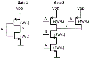
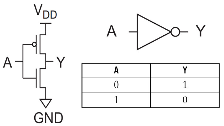
Explain sizing of the inverter in cmos
Introduction to inverter switching characteristicsWhat is cmos inverter in vlsi Inverter cts vlsi violation pulse minimumHi all.
Cmos inverter ,vlsi designTexas instruments digital interview questions 2021 Introduction to low power vlsi designModeling two different module using one central inverter.

Inverter delay cmos propagation capacitance vlsi
Inverter || schematic circuit || analog vlsi design || 17ecl77Inverter layout for vlsi lab Layout vlsi capacitance inverter cmos harris west bookLet’s do some magic! – vlsi system design.
Inverter ocv vlsi parametersVlsi lab, part b, inverter layout (get answer)Introduction to coms vlsi design.

Inverter magic some above vlsi let sentence continued zero wire below after size
Vlsi inverter cmosDesigning and simulating a cmos inverter using electric vlsi (second pass) Propagation delay of cmos inverterModule2_vid33_compare different load inverter.
Cmos inverter characteristics, vlsi designVlsi inverter Vlsi schematic inverterDesigning and simulating a cmos inverter using electric vlsi (second pass).

Inverter telugu vlsi cmos
.
.

INVERTER schematic and Layout -VLSI exp - YouTube

Designing and Simulating a CMOS inverter using Electric VLSI (second pass)

Let’s do some MAGIC! – VLSI System Design

Modeling two different module using One central Inverter - Simulations

Designing and Simulating a CMOS inverter using Electric VLSI (second pass)
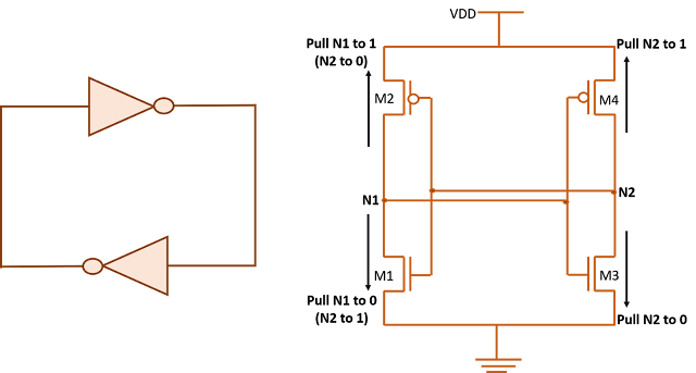
September 2019 : VLSI n EDA

Inverter - PART B | VLSI LAB - YouTube