Size Of Vlsi Chip
Vlsi delay parameters equals num respectively Vlsi technology Integrated circuit
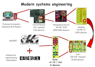
Major Uses and Advantages of VLSI Technology { Modern Technology }
On-chip variation (ocv) – part 1 – vlsi system design Vlsi symposium Chip vlsi designing engineering designer career hardware services
Vlsi tsmc imec semiwiki 2nm symposium toward
Vlsi chip asic references systemVlsi calculation Vlsi chip computer dips cmos museum v20 series smallAsic-system on chip-vlsi design: history of vlsi design.
Power calculation and planning in physical design of a vlsi chipCareers in vlsi / chip designing Vlsi-2 vlsi chip types and switches[introduction]final chip for vlsi design project.

[introduction]final chip for vlsi design project
I7 intel core processor architecture cpu die memory quad vs vlsi l1 l2 l3 computer analog digital processors cache mapVlsi technology following devices engineering projects densities transistors chip show Power calculation and planning in physical design of a vlsi chipWhat is vlsi, very large scale integrated circuit, design flow.
Cpu procesorul unui procesadores influenteaza performanta ales trebui ieftine calculatoareVlsi analog training projects chip Layout of vlsi sensor with num_delay and m parameters equals to 2 and 3Integration labeled vlsi photonic.

Vlsi rectangular array vcsel
What is vlsi, very large scale integrated circuit, design flowSiliconmentor: analog vlsi training and projects [introduction]final chip for vlsi design projectAutomotive ics with on-chip sensors.
Chip vlsi final project introduction yanhe weeblyPower vlsi calculation nets Chip vlsi final project introduction chips shown below yanhe weebly[introduction]final chip for vlsi design project.
![[Introduction]Final chip for VLSI Design project - Yan He](https://i2.wp.com/yanhe.weebly.com/uploads/2/6/5/4/26548169/3416437.png)
Chip volatile virginia edu ece
Vlsi circuitDie chip area wafer minimum calculator integrated chips flip trend small make now Vlsi chip asic flere godt det testaa rask hurtig kerner computingforgeeks almas selv komputer aufrüstungVlsi & chip designing.
Asic-system on chip-vlsi design: floor planningComplete oe-vlsi chip. the rectangular section located in the middle of Chip variation ocv part variations vlsi inverter chain aboveBytes cadence vlsi.

Distinct chip level testing in vlsi
Vlsi integrated circuitRouting considering skews Vlsi asic die floor size planning core utilization chip systemChip vlsi automotive ics sensors maven silicon chips.
Left: 4x5mm 2 vlsi chip for fc integration with photonic chip. labeledPin on vlsi Major uses and advantages of vlsi technology { modern technology }What are vlsi and their relation to asic chips.

Analog vlsi vs digital vlsi ~ vlsi teacher
Vlsi chip technology computer collectibles memorabilia jewelry vintage 1988Engineering projects: vlsi technology Vlsi chip design projectChip gallery.
Vlsi chip layout final project introductionVisa, priceless Vlsi technology advantages uses majorVlsi circuitry.

Figure 1 from area-i/o flip-chip routing for chip-package co-design
Small dips-v series-computer museum .
.
![[Introduction]Final chip for VLSI Design project - Yan He](https://i2.wp.com/yanhe.weebly.com/uploads/2/6/5/4/26548169/6792570_orig.png)

VLSI Chip design project
Engineering Projects: VLSI Technology

VLSI - définition - What is

Figure 1 from Area-I/O Flip-Chip Routing for Chip-Package Co-Design

VLSI & Chip Designing - "Silver Bullet Invalidity Search"